If you are considering this question chances are you are designing a radio receiver for a narrow band communications system. Crystal filters are sometimes used in transmitters as well, in a super heterodyne (superhet) transmit chain, to clean up the modulation spectrum and reduce adjacent channel noise. The same arguments apply here as for the receive case.
Achieving a narrow receive bandwidth
There are several options elaborated here.
SAW filters
At the wider end of the narrowband range SAW filters are usable and offer higher IF frequencies than crystal filters, so making it easier to achieve good image rejection in a superhet receiver. However for the narrower range, the available bandwidths are not small enough. There are two reasons for this. One is the available Q factor of a SAW resonator, abut 2k typical, whereas a crystal achieves typically 100k. The second is temperature stability. A crystal filter follows the AT cut crystal temperature drift characteristic so the shift in centre frequency can be kept within ±20ppm or better over the usual temperature ranges. Narrow SAW filters follow a XT cut characteristic similar to that of a tuning fork crystal. Over -40⁰C to +85⁰C this gives a potential -189ppm shift in the filter centre frequency. This has to be allowed for by making the passband wider. This in turn reduces the adjacent channel rejection achievable.
If your receiver has a wide tuning range over the HF and/or VHF spectrum then an up-conversion superhet architecture should be considered. Narrow SAW filters in the UHF range such as Golledge MA05334 (119.64MHz CF, 30kHz BW), or MP06905 (469.8MHz CF, 710kHz BW) make an excellent 1st choice. For this architecture the front end filter can be a low-pass greatly simplifying the front end design.
Ceramic filters
For a long time this was the preferred way of achieving tight selectivity and narrow channels. This comes at the expense of higher complexity, as often a double conversion architecture (with a crystal filter at the first IF) is required to get to the 455kHz IF while achieving good image rejection. The performance disadvantage of this approach is that placing the main selectivity further down the receiver chain compromises the blocking performance. The added complexity also brings extra current consumption and cost in the receiver circuits. This design approach is now out of favor, and ceramic filters are getting harder to buy, following the main supplier’s withdrawal from the market.
LC filters
The low Q of practical inductors makes achieving narrow filters only feasible at low IF. The same problems as the ceramic filters then apply.
Zero IF
This approach has become increasingly popular in recent years with the availability of cheap ADC and DSP devices. High dynamic range and good adjacent channel rejection are possible. The image rejection problem goes away, but is replaced with the need to maintain good quadrature and amplitude control of the two LO and IF paths. Tighter control of filter shape is possible than with analogue techniques, making this suitable for complex signalling techniques that are not tolerant of variations in group delay characteristics. All this comes at the expense of complexity, cost, and the high power consumption of analogue to digital converters and the DSP. Two front end mixers are also required with quadrature LO feed to provide the I and Q signals needed to resolve positive and negative frequencies. There is also the difficulty in removing DC offsets, requiring either a notch in the centre of the receiver characteristic from having a high pass filter in the baseband signal chain, or periodic self calibration to remove the DC offset. As the IF is spread across low frequencies 1/f noise in the baseband circuits gives a poor IF noise figure. This limits the receiver sensitivity, or requires more frontend LNA gain to compensate. Having more LNA gain compromises the receiver dynamic range. Local oscillator leakage from the antenna port is also a problem as the LO is at the wanted frequency so cannot be removed by the frontend filters. Another gotcha is that if you have commutating mixers for the down conversion to achieve good dynamic range, then the front end filter needs to have good rejection at the 3rd harmonic, and above, as the mixers will mix down the odd harmonics very effectively giving the receiver spurious responses.
Direct sampling
This is very similar to the Zero IF approach except that the A to D convertor is before the mix to Zero IF, and following lowpass filtering happens using digital processing. The advantage of this is that it eliminates the DC offset and baseband noise issues. The problem is that the very high sample rate and dynamic range required of the ADC makes this a very power hungry and expensive solution. The high data rate from the ADC also requires a FPGA or dedicated digital down converter to do the down conversion, low pass filtering, and decimation to produce a sample rate that a DSP chip can handle.
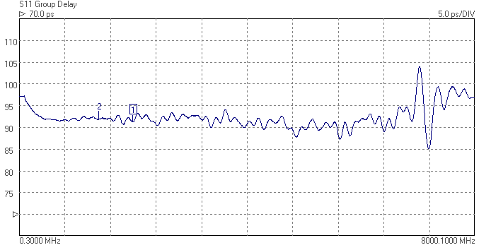
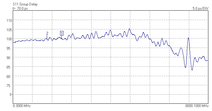
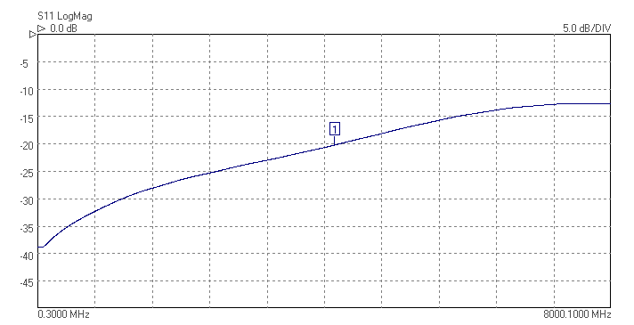
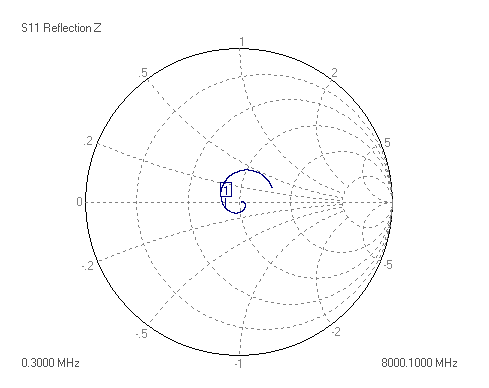
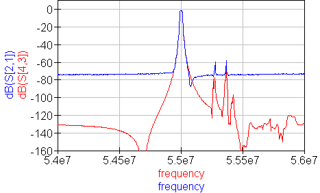
Crystal filter
The superhet receiver architecture has a well established history. Crystal filters have the advantage of excellent signal handling range, low loss, tight selectivity, and being passive, no current consumption. They are also low cost. Advances in packaging mean that, unlike in the past, parts are available in modern surface mount packages that do not take up too much PCB area. Advances in manufacturing techniques mean that higher IF center frequencies are now possible making achieving good image rejection easier. 45MHz is now the new normal for crystal filter based IFs, and 70MHz is becoming increasingly common. Of course there are weaknesses, if a high shape factor is needed than a crystal filter with a large number of poles is required and hence a larger through hole package. The termination impedances are high, but BSL can help with this by suggesting suitable matching networks should working in a 50 ohm system be needed. There is some variation part to part and over temperature, but modern manufacturing process control mean these are minimized. Some of the highest performance narrow band receivers use a hybrid of crystal filters and digital filters to get the best of both worlds. The precision and sharp cut-off of the digital filter but allowing lower sample rate and needing fewer bits resolution in the ADC after the crystal filter, saving considerably on cost and power consumption.